 EN
 IT Italiano
 ES Español
 FR Français
 DE Deutsch
Description
What it is
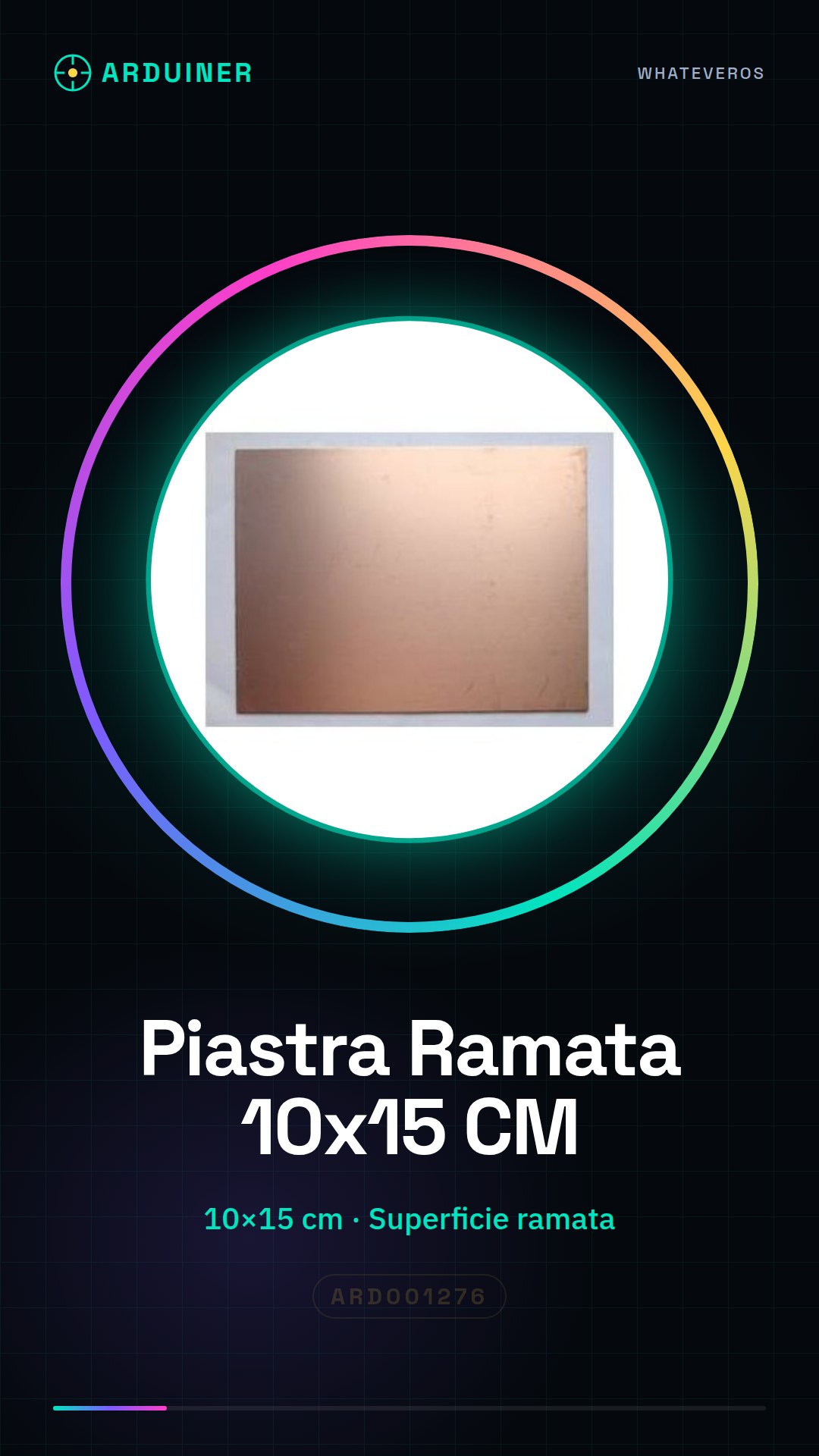
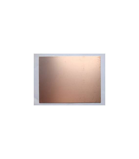
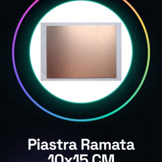
The single-sided copper-clad board measuring 10×15 cm is an essential component for makers and electronics enthusiasts who want to create custom printed circuits. This PCB base offers a copper surface on one side, allowing for the creation of prototypes and projects with high flexibility.
Features
- Size: 10×15 cm
What it is for
Ideal for creating simple lighting circuits, small and medium-sized projects. It can be used in combination with Arduino or ESP to create functional prototypes.
Tutorial: How to Use Single-Sided Copper Clad Board Size 10 * 15 CM
The single-sided copper-clad board is a fundamental component for makers who want to create custom printed circuits. This type of board is ideal for both small and medium-sized projects and allows beginners and intermediates to create professional PCB designs.
What you need
- file
- ferric acid
- protective board
- laser printer
- thermal transfer printer
- etching kit
Steps
- Print the circuit layout on paper using a laser printer. Check the datasheet for resolution and print quality.
- Place the printed paper over the copper clad board, ensuring it is centered. Use a thermal transfer printer to transfer the image onto the board.
- Gently remove the paper from the PCB using hot water and a soft cloth.
- Etch the copper clad board in ferric chloride. Check the datasheet for the correct etching times.
- Once etching is complete, thoroughly wash the PCB with cold water until all protective coating is removed.
- Use a scraper to remove any remaining coating and clean the copper clad board with isopropyl alcohol.
- Prepare the holes for the resistors, capacitors, and other components using an appropriate tool such as a drill or needle.
- Check the entire PCB to ensure that all lines are clear and there are no short circuits.
Mini project
Create a simple lighting circuit with LEDs, resistors, and a button on this copper board. The project should take approximately 30 minutes.
Common mistakes
- Do not use colored printer paper or light-sensitive photo paper.
- Leaving the PCB in ferric chloride for too long, causing excessive removal of copper.
- Not cleaning the PCB thoroughly after etching, leaving residues that can interfere with components.
- Using a thermal transfer without first applying a protective board.
Recommended accessories
- Etching Kit
- Thermal Transfer
- Scraper
- Ferric Chloride
Frequently asked questions
How can I protect the PCB after it is made?
Use a protective spray to apply moisture and corrosion resistant paint.
Can I use any printer paper with this method?
No, it is recommended to use laser printer paper specifically for transferring to PCB.
Reviews
There are no reviews yet.