 EN
 IT Italiano
 ES Español
 FR Français
 DE Deutsch
Description
What it is
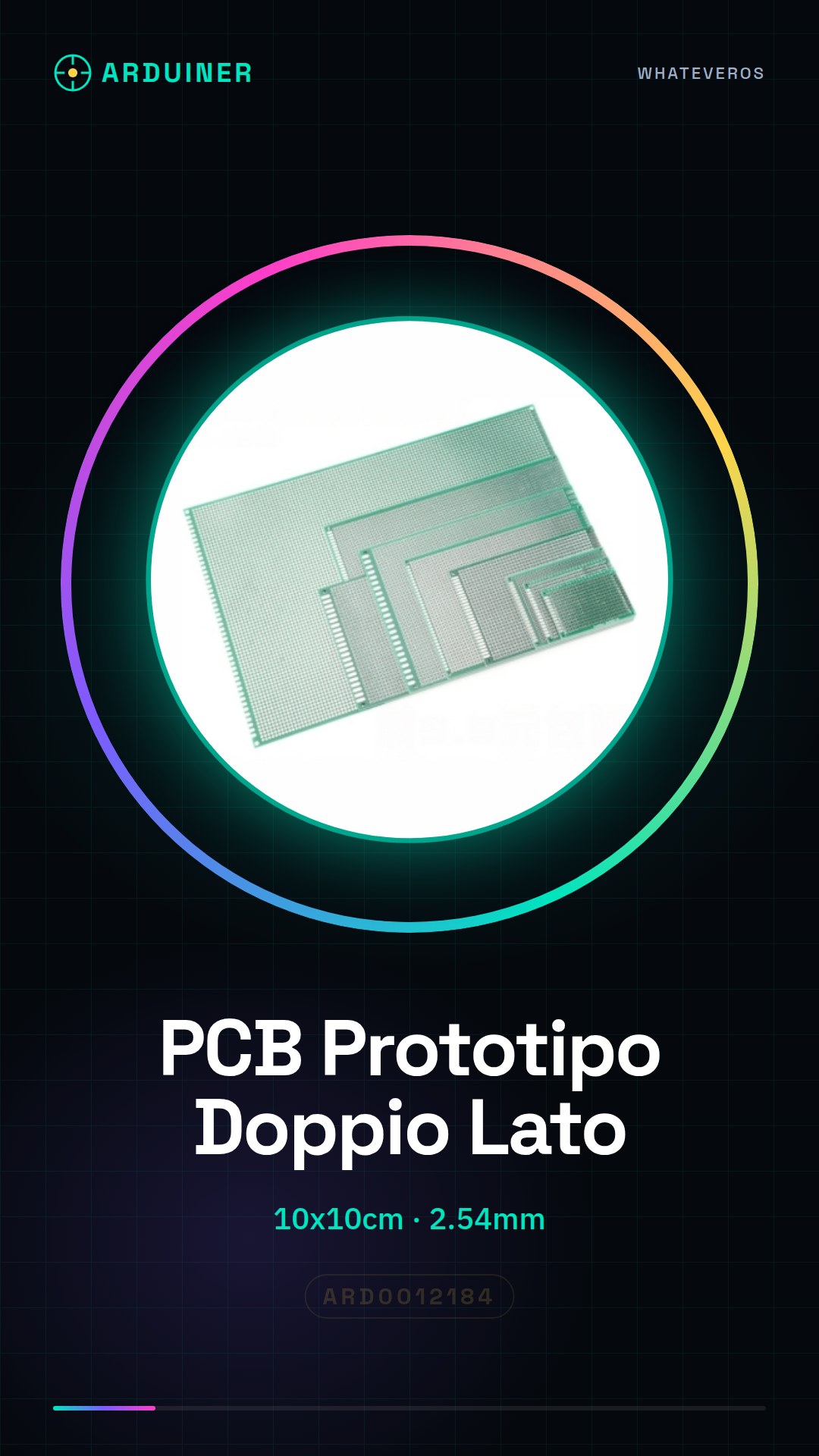
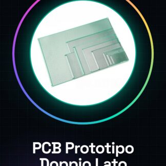
The Double-Sided PCB Prototype 10x10cm 2.54mm is a standard-sized printed circuit board prototype, ideal for makers and students who want to test and develop electronic projects. This PCB allows for the quick creation of electronic circuit prototypes without the need to produce a final PCB.
Features
- Dimensions: 10x10cm
- Pad spacing: 2.54mm
- Double-sided
What it is for
This PCB can be used for various types of projects, such as creating simple LED lighting circuits with resistors, connecting sensors and input/output devices, and testing circuits with Arduino or other microcontrollers. It is a fundamental component for those learning to work with printed circuit boards and for those developing electronic project prototypes.
Tutorial: How to use Double-Sided PCB Prototype 10x10cm 2.54mm
The Double-Sided PCB Prototype 10x10cm 2.54mm is essential for makers who want to test and develop electronic projects. This PCB is perfect for those learning to work with printed circuits or for those developing a prototype.
What you need
- laser printer or photopolymerizer
- protective film sheet
- ferric chloride solution
- copper board
- iron
- insulating board
Steps
- Step 1: Draw your electrical schematic on software like Eagle or Fritzing.
- Step 2: Print your layout on a laser printer or photopolymerizer using transparent paper.
- Step 3: Apply the protective film on the printed side of the transparent paper.
- Step 4: Use the iron to transfer the layout onto the copper board.
- Step 5: Remove the transparent paper and the protective film.
- Step 6: Immerse the copper board in the ferric chloride solution to remove the unprotected copper.
- Step 7: Clean the PCB with water and soap to remove any remaining ferric residue.
- Step 8: Use a toaster oven or an iron to solidify the PCB, then you can start soldering the components.
Mini project
Create a simple lighting circuit with an LED and a resistor. Connect the LED to the PCB and test the circuit with an Arduino.
Common mistakes
- Do not use a laser printer, but a photopolymerizer to achieve a more precise transfer.
- Do not apply enough pressure with the iron during the layout transfer.
- Do not clean the PCB completely before soldering.
- Do not use a toaster oven to solidify the PCB, which can cause soldering problems.
Recommended accessories
- Laser printer or photopolymerizer
- Ferric chloride solution
- Iron
- Insulating board
Frequently asked questions
How can I protect the PCB after it is made?
Use a protective lacquer to cover the PCB and prevent oxidation.
What tools are necessary for soldering?
A soldering iron, a set of pliers, and a set of probes.
Can I use this PCB for long-term projects?
The PCB prototype is suitable for testing and development, but for long-term projects it is recommended to use a PCB manufactured by a professional manufacturer.
Reviews
There are no reviews yet.